In 2007 GMC introduced the second redesign of Cadillac Escalade.
 Performance
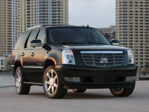
2007 AWD Escalade shares new platform GMT 900 with GMC Tahoe and Yukon, has got standard stability control, and attractive grille and headlights. One of the main problems with Escalade is its sticker price: base model starts at $ 56,405 in the USA, and options may add another 10,000 dollars to the price-tag.
Information package
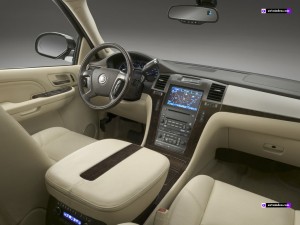
Escalade owners prize highly its information package that includes touch-screen navigation, rearview camera and Intellibeam. Kids will enjoy rear-seat entertainment system with 8-inch tilt-down screen DVD players, 10-speaker Bose 5.1 Dolby Digital and 2-channel wireless headphones. Surprisingly, Cadillac doesn’t offer Bluetooth phone integration, and only recognizes some 40 voice commands.Escalade interior
 Interior
Majority of owners reports satisfactory Cadillac Escalade 2007 impressions. The huge cabin of Cadillac Escalade offers 3 rows and enough room for 7 people. Dark ebony seat leather, wood and aluminum add to the luxury status of the vehicle. Luxury addition to your Escalade is a large sunroof and 22-inch chromed aluminum rims.
2007 Cadillac Escalade is equipped with 6.2-liter engine, and is available with manual or automatic transmission. No surprise, Escalade won 5 stars in NHTSA frontal crash-test; however it only got 3 stars for rollover protection. The 2007 Escalade is offered with 4 year or 50,000-mile warranty.
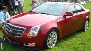 Stylish Cadillac CTS is one of the most successful vehicles by Cadillac. It is considered as one of the best midsize cars on the market today.
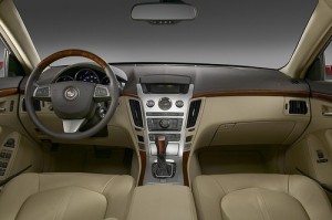 Cadillac CTS reviews highly prize Cadillac Premium Care program, that covers scheduled maintenance for 50,000 miles or four years.
 GMC takes over